As PCB layouts are becoming increasingly dense, causing antennas to face the persistent and often overlooked challenge of detuning caused by nearby components. Design engineers are under pressure to minimise board size and integrate more features whilst guaranteeing reliable connectivity at the same time.
This balancing act often brings antennas into close proximity with batteries, shielding components, displays and other conductive elements, all of which can shift an antenna’s resonance and degrade performance. So how can designers anticipate and mitigate detuning when every millimetre of board space counts?
What is detuning?
Detuning occurs when the resonant frequency of an antenna shifts away from its intended operating band. This happens when surrounding components or even the enclosure itself alter the electromagnetic field around the antenna. The results are reduced efficiency, poor impedance matching, and in severe cases, complete communication dropouts.
For example, a GPS antenna placed too close to a large battery may shift out of band, compromising its ability to reliably connect with satellites. Similarly, a smart meter antenna encased in plastic or surrounded by metal shielding may lose significant performance if detuning isn’t considered early in the design.
Common causes of detuning in crowded PCBs
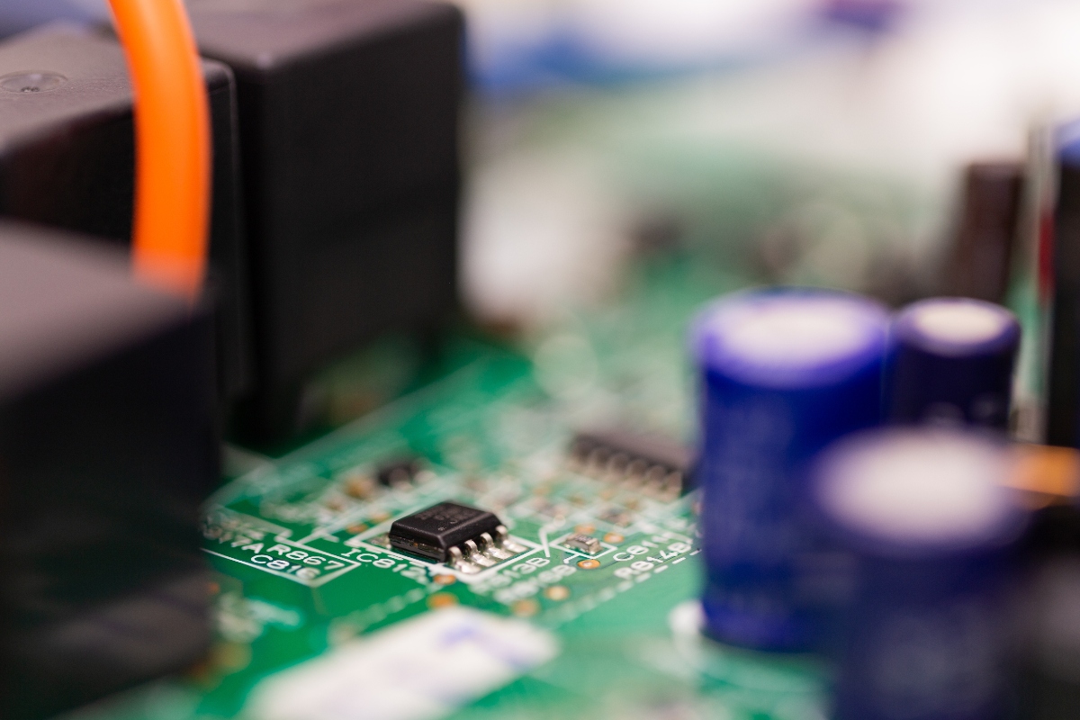
When working with dense PCB layouts, detuning rarely comes from a single source. Instead, it’s usually the result of several interacting factors within the device environment. Understanding the most common causes of detuning is the first step toward designing strategies that protect wireless performance.
- Metallic components: Batteries, shielding cans and heatsinks absorb or reflect RF energy.
- Ground planes and traces: PCB layout choices can alter the current distribution around the antenna.
- Enclosures and housing: Plastic, metal or even glass can all affect RF propagation differently.
- Other antennas: Multi-radio designs (e.g., LTE + GNSS + Wi-Fi) risk mutual coupling if not isolated properly.
Design strategies to minimise detuning
Detuning can’t always be completely eliminated, but its impact can be managed with the right design approach. By considering the antenna’s environment early and applying proven best practices, engineers can significantly reduce interference and maintain reliable wireless performance.
1. Plan antenna placement early
Antenna design cannot be an afterthought. Integrating wireless performance into the product design phase (rather than post-layout) prevents costly redesigns and compliance failures.
2. Maintain clearance
Follow the antenna manufacturer’s recommendations for keep-out zones. Even a small conductive trace too close to the antenna feed can shift performance dramatically.
3. Use high-performance embedded antennas
Modern embedded antennas are designed with integration in mind, offering predictable performance even in compact spaces. Selecting a part optimised for confined layouts reduces risk.
4. Tune for the real environment
Always validate antenna performance inside the final housing, with all components in place. Detuning often only becomes evident in the full product assembly.
5. Leverage matching networks
A carefully designed matching circuit allows fine-tuning of antenna performance to counteract minor detuning effects introduced during assembly.
Choose the perfect antenna for your device
As PCBs grow denser, detuning is an unavoidable reality but not an unsolvable one. With early planning, careful component placement and the right antenna solutions, engineers can mitigate interference and deliver reliable connectivity across even the most space-constrained devices.
At Antenova, we design antennas that are compact, efficient and resilient to the challenges of crowded PCBs. Our products are engineered to simplify integration and shorten design cycles, helping designers achieve reliable performance without compromise.
From GNSS modules optimised for asset tracking to antennas tailored for smart meters facing high levels of signal absorption, we provide solutions that work with your design constraints, not against them. Check out our full line of antenna solutions here.
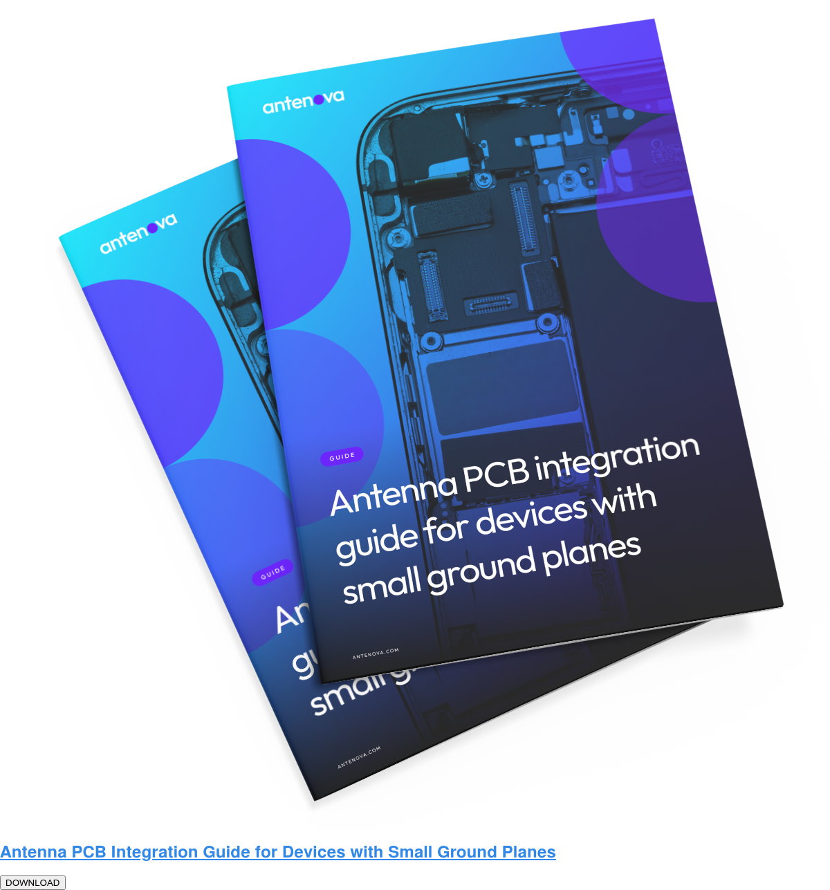
To find out more about integrating antennas onto devices with limited PCB space, download our guide below.