
New wireless technologies are changing the world around us. From video conferencing to street lighting and coffee machines, wirelessly connected SMART devices are driving better communication between both humans and the tech that makes our lives easier.
Coming up with the next great wireless device is one thing, but knowing how each component of a design will interact and impact performance is quite another. Architecture layout is the phase of design where the best layout of the device is decided, sometimes using behavioural models to judge how each component will work alongside one another, and subsequently how to get the optimal performance from them.
An improperly designed architecture can be catastrophic for wireless antennas, with issues ranging from impedance mismatch right up to signal radiation, both of which can cause efficiency loss and even a loss of communication. So what should designers keep an eye on at this crucial point of the wireless design cycle?
Power management
There is a simple rule of thumb in RF: the more data a device has to communicate, the more power it will consume. Thus lower data rates will drastically conserve power. This is of particular importance for devices that rely on battery power, especially when the ever-shrinking nature of modern technology often means antennas will have to sit near the battery, which can cause frequency shifts during use.
Similarly, the voltage and performance of a battery can affect antenna performance. For instance, an unstable supply or fluctuations in voltage might lead to distortion, or even a complete signal drop out if a voltage should become too low. As such, alkaline or lithium single-use batteries are often preferable because of their voltage stability.
One option for designers that only require small data transfers from their devices is Narrowband IoT, a low power wide area network (LPWAN) technology that has been developed to make communication more efficient and save power consumption. Under the right conditions, NB-IoT can even deliver up to 10 years worth of battery life.
If battery life is an important spec for a device, then careful RF integration is essential. The better the design, the greater efficiency an antenna can perform at. This is simply because the time needed to transmit and receive data is reduced. Transmitting and receiving data takes energy, and a more efficient design reduces the amount of time it takes to process this data. Less efficient designs take longer to process smaller chunks of data, which can eat into the longevity of a battery.
Stability and reliability
Even the smallest and most technologically advanced antennas are dependent on fairly exact parameters to achieve their incredible capabilities. The best way to ensure optimum operation is to follow the design-in guideline that each antenna comes with, most usually supplied in the data sheet.
Chip antennas have become a preferred option due to their design flexibility and ability to negate detuning effects, but they require certain architecture fundamentals to be in place. Certain designs like stacked PCBs might not allow for a ground plane that conforms to the design guidelines – and so knowing the impact this architecture will have on your components will mean the difference between a optimisation and loss. Yet there are a variety of antennas available which could prevent the need to rethink your layout, such as FPC antennas.
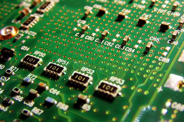
Circuitry performance
A final consideration while laying out the architecture is to match networks, by marrying the source impedance to the load impedance. Matching networks allow an antenna to radiate at the intended frequency with minimal deviation, vastly increasing performance capabilities, maximising power transfer and reduce losses (VSWR).
Many engineers favour a three element pi matching circuit (five element, in the case of multi-band 3G/LTE antennas) as it uses only a few components to correctly match an antenna to its source impedance. This means a pi network can be matched to almost any load conditions while still being re-tuneable throughout the design process.
This may seem a lot to plan for a device’s architecture layout. But from the relationship between the power supply and antenna frequency to knowing the design fundamentals of your components and how to match them, this is a crucial step for your product. Fortunately, all of Antenova’s antennas are designed for integration and come with clear guidelines for installation. For more information on finding the right antenna for your design, check our guides on RF data sheets.