
When designing compact devices, the devil is in the details. However nimble and well-placed each component is, a minor issue can result in a failure to deliver on-brief. PCBs are complex, lots of hard work goes into configuring multiple parts side by side; often leaving precious time to consider your antennas impedance matching and trace line dimensions.
Impedance matching is vital to the overall performance of your device. If executed accurately, impedance matching ensures your devices antenna is receiving as much of the wave energy as possible. A well-matched antenna can result in an antenna performing with nearly 100% efficiency.
The importance of impedance matching
Impedance matching is, in simple terms, ensuring that a trace lines’ dimensions propagate the effective transmission of RF signals from load to source. The dimensions of transmission lines affect its characteristic impedance. The correct dimensions properties, therefore, ensure the characteristic impedance of a transmission line matches the load impedance - meaning that the load absorbs the wave energy maximally.
Failure to do this accurately could result in your devices’ antennas receiving a partial amount of power from the amplifier, this means the transmission lines will suffer losses which reflect back to the antenna and detune it. If this is the case, your device may fail to function, or perform inefficiently.
Without proper impedance matching, you cannot guarantee a device will perform as expected; an outcome that could cost the manufacturer dearly in delays or even lead to a product recall. Having to redesign a device due to an inaccurately drawn trace is an easy, but costly mistake.
With the time and money that goes into designing modern products, it pays to be confident that your transmission lines match impedances optimally.
What are transmission lines?
Using transmission lines makes it possible to transfer RF energy from one place to another with minimal losses. In larger applications, a transmission line can come in the form of a coaxial cable; but in smaller circuit board designs with embedded antennas, we recommend using a grounded coplanar waveguide.
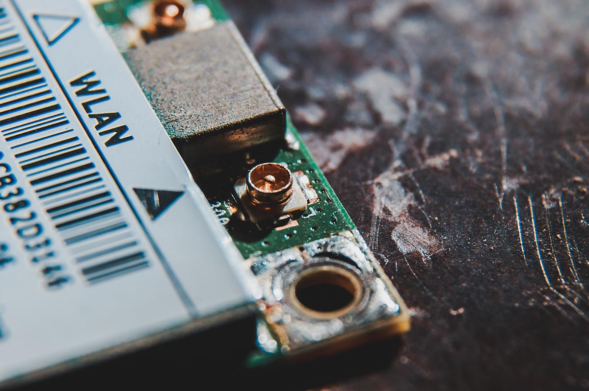
A grounded coplanar waveguide is a type of transmission line which is often utilised for very small applications. It sits in ground-signal-ground configuration on the top layer of a circuit board, with an additional ground plane beneath the signal.
Made up of a conductive strip, surrounding ground planes, isolating gaps, and a dielectric substrate layer; a major benefit is that each of its many elements can be modified in terms of their dimensions and spacing between one another. This makes grounded CPWs well-suited to impedance matching as their extra dimensions make for more accurate impedance matching as well as requiring less real estate on the PCB.
Reflections: they're problematic
RF signals move from the output of one component to the input of another component; for example from a power amplifier to an antenna. An RF signal, however, is not a one-way communication; much like a wave hitting a stonewall, signals bounce back. This redirection results in signals travelling back from the load towards the source, otherwise known as a ‘reflection’.
Reflections greatly reduce an antenna’s efficiency as a portion of the output power is reflected back to the amplifier. This causes losses, which will reduce the performance of an antenna by as much as half.
Antenova’s free tool calculates transmission line dimensions for optimum impedance matching
To prevent reflections it is necessary to match the load impedance to the characteristic impedance of the transmission line.
With PCBs becoming more complicated, designers don't want to spend too much time drawing a single RF trace line when they have the whole board to complete. But at the same time you don’t want a device with potentially poor RF performance because of a poorly designed trace.
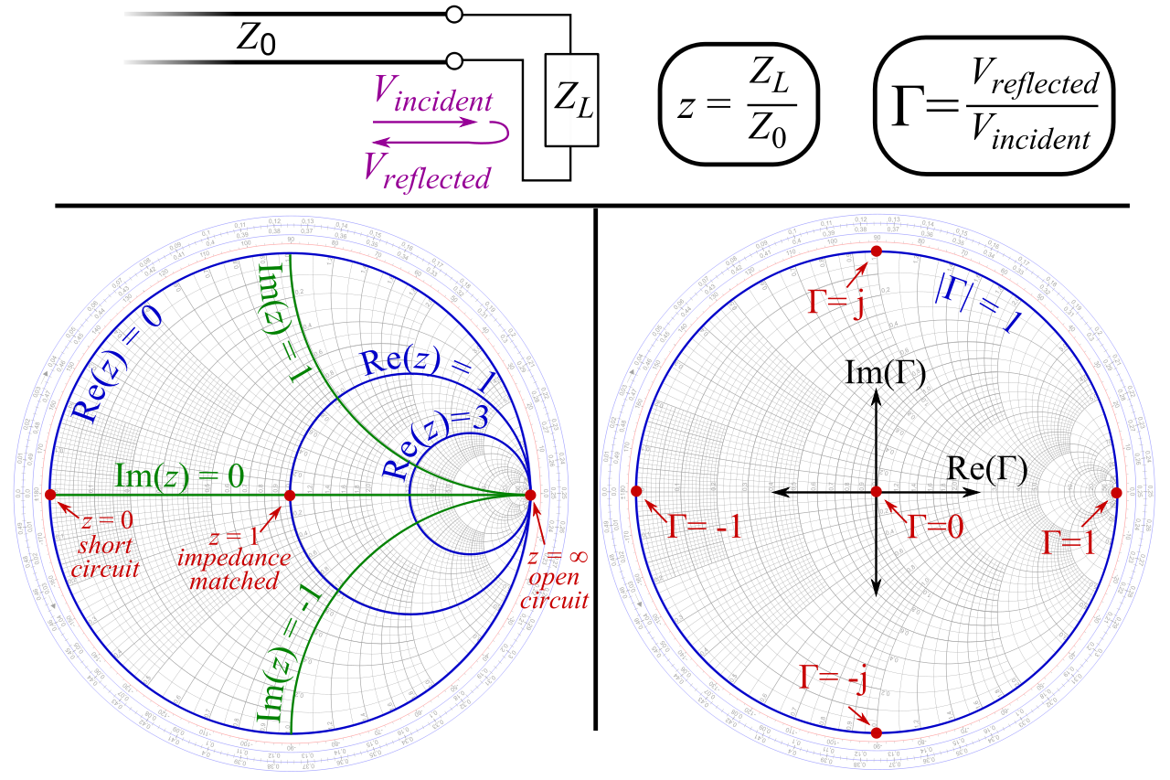
Using traditional methods, trace line calculations involve multiple time-consuming processes, using complicated formulae and Smith charts, which offer limited assurances in terms of accuracy if rushed.
With Antenova’s free Transmission Line Calculator it is possible to calculate the optimum dimensions of your transmission line to achieve maximum efficiency, with complete accuracy, in just a few seconds.
By inputting the dielectric constant and height of your PCB, a graph appears displaying the relationship between the gap and width of the waveguide - it then plots dimensions which show different possibilities that will give you an accurate 50 ohm match.
With these options, you can decide on measurements depending on the constraints of the design your working on. This means, no matter how small a device, its transmission lines will be drawn accurately.
By drastically reducing the time it takes to draw trace lines, and by assuring designers that the dimensions of the trace match impedance accurately; our trace line dimensions calculator offers a convenient tool for delivering optimal antenna performance.