Integrating an antenna is a crucial step in a wireless product design. Antennas behave differently to digital integrated circuits (ICs). This creates a unique set of design challenges and considerations that traditional design cycles do not account for.
With devices getting smaller, designs are becoming intrinsically less RF-friendly. Circuit boards are shrinking, yet are tightly packed with noisy components. An antenna cannot be simply ‘added’ at the end; RF must be a priority from the outset.
More product designers are facing this challenge. To design great wireless products, designers need to change their approach. Our proven cycle considers wireless design first, and it’s suitable for projects of all scopes and sizes. Here’s how we recommend that you approach your wireless product design.
The wireless product design cycle
- Research
- Architecture layout
- Board design
- Gerber review
- Design test
- Pre-production
- Mass production
Research
The wireless design cycle starts at the same time a design project does. Wireless technologies are the enablers of connectivity and there’s lots of them. Likewise, antennas are also available in a variety of forms. Designers that are aware of the variety of options available will be more empowered to fulfil a brief.
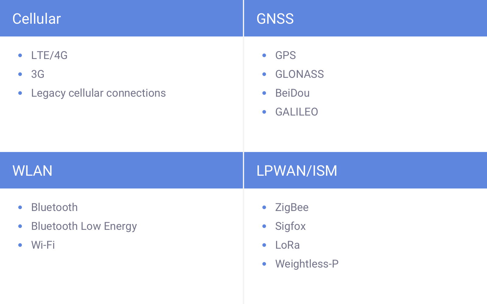
Wireless technologies
There are wireless technologies available to suit any sort of device. Whether you require long-range connectivity without large power requirements, or precision tracking, there is sure to be a technology to suit:
While selecting a technology, there are a number of factors to consider:
- Data throughput. How talkative will your device be? Will it require tens of megabytes or just a few bytes?
- Range. How far away will the device be from the base station?
- Power consumption. How much life should your battery provide?
- Certifications. To launch a device on a cellular network, you will need to pass all of the relevant certifications. In North America, the performance of an antenna will be intensely scrutinised. The region has some of the toughest passing criteria for certification globally.
There is no one-size-fits-all wireless technology. The right choice will depend on data throughput requirements, range, power consumption and certification needs. More designs are incorporating multiple wireless technologies, too. This makes the choice of complementary antennas crucial.
Antennas
It’s the antenna that makes it wireless. Antennas are therefore crucial components in the Internet of Things. The diversity within IoT reflects the availability of antennas; antennas in a huge variety of configurations are capable of connecting devices.
For a deeper look at the different types of antenna, and the benefits and drawbacks of each, download our Wireless Antennas: Compared guide.
Surface-mounted antennas
Surface-mount device (SMD), sometimes known as surface mount technology (SMT), antennas are far and away the most popular type of antenna available today. These mount directly to the PCB, and come in a variety of shapes, sizes and materials.
These are commonly available in high-grade dielectric laminate substrates, ceramic, or even stamp metal. There are some advantages that come with their use:
- SMD antennas are tiny. Some antennas measure just a few millimetres.
- They are low-cost and easy to assemble using pick and place equipment.
- Within a compact form, they offer high levels of performance.
As SMD antennas are inexpensive, yet offer great performance within a compact form, their popularity is logical. However, to enable a surface-mounted antenna to perform well, the design must be optimised.
RF Modules
Like an SMD antenna, modules can be placed directly on the PCB. The advantage these have over standard surface-mounted antennas is that they come pre-assembled. The antenna will already have a chip and other key components.
These work excellently for GNSS applications. They effectively offer a ‘drop-in’ solution, which means that designers do not need to spend time designing in complex RF circuitry.
Our friends at Digi-Key have an excellent article covering the major design considerations when using antenna modules. The article features the Antenova RADIONOVA module M20050-1.
Case-mounted antennas
For applications that require tiny circuit boards, surface-mounted solutions are not always the most appropriate antenna solution.
And, for applications that use non-RF friendly materials – like metal – it will always prove difficult to achieve strong wireless performance levels with an embedded antenna.
Antenova’s patented REFLECTOR technology isolates case-mounted antennas from noise. By using a layer of material for isolation, the antenna can perform with minimal losses, even when mounted on metal.
With just a single connection to the circuit board, these antennas do not require ground plane space on the circuit board. This frees up space for other components. It also means the designer is more free to place switches and other noisy components where is most convenient.
Flexible printed circuit board (FPC) antennas
As space-saving antennas go, FPC antennas are probably the best. These antennas have an extremely low profile yet offer unparalleled design flexibility.
FPC antennas are commonly deployed within wearables and small handheld devices. They can wrap around the housing of a device, all while connecting to the circuit board via a single UFL connection.
Antenova’s flexiiANT antennas are available in a variety of connection-types and cable lengths to enable their use within ultra-compact devices.
Architecture layout
Antenna placement
With any antenna, understanding where it’s placed will impact how it performs is essential. Particularly for an embedded antenna, the antenna needs to be positioned clearly away from the rest of the circuit – otherwise noise and other components can detune and impedance performance.
Most antennas perform best when positioned on the corner of the PCB. However, there are some antennas that operate best along the long-side edge. The data sheet of each antenna will detail the optimum placement of the antenna, as will the design of the evaluation board.
The gap between the casing/housing and the antenna is also an essential consideration. Plastic has a higher dielectric constant than air, so placing an antenna too close to it is likely to detune the signals.
We’ve written an article that covers all of the essential considerations for placing your antenna.
Board design
Placing the antenna on the circuit board should be the first step in your board design. Antennas may be the only component that must be located in a specific physical position on the circuit board. This means you’ll need to consider:
- Ground plane size. Antennas use ground planes in order to radiate efficiently. In an antennas datasheet and EVB, there will be a recommended size of ground plane. This is not a minimum, but an antenna will perform less well under these circumstances.
- Component layout. Position noisy and metallic components away from antennas, where possible.
- Antenna coexistance. Plenty of wireless product designs harness multiple wireless technologies.
- Casing material. Metal housings are not conducive to RF performance. As well as the material of the casing, screens, batteries and metallic buttons can have RF implications. Position these away from antennas as best as possible. There are different solutions if the product requires a metal casing.
- Position RF circuitry within the vicinity of the antenna. Longer transmission lines are more prone to reflections and signal losses. This can reduce performance drastically – as much as 50% of RF energy can be lost through a transmission line.
Antennas have unique keep-out requirements. Some suggest certain keep-out zones which should be free of any components.
Gerber design review
Prevention is better than cure. Following the completion of the first version of a board design, the designer can make a number of checks to ensure wireless performance is well optimised. There are several key questions to address.
Transmission Lines
- Does the device use a suitable transmission line?
- Does the impedance of the transmission line match the source and RF circuitry?
- Are transmission lines short and without corners (i.e. using chamfered edges where possible)?
Matching circuit
- Have you incorporated a matching circuit (such as a Pi matching circuit) within your RF circuitry?
- Do the values of your matching circuit enable an impedance match?
Via placement
- Usage: Are vias used to form a ground fencing?
- Spacing: The spacing between two vias should exceed 5% of the wavelength of the RF signals.
- Separation: Are separate vias used for each pin and pad?
Design test
Verifying a device operates as expected in the hands of consumers is a step not to be missed. In fact, all cell carriers and network operators will conduct testing on devices that are to launch on their network. In North America, due to geographic reasons, this testing is extensive – and the passing criteria is renowned for being difficult. 3 out of 5 devices are thought to fail certifications at the first attempt.
Not everyone has access to sophisticated anechoic testing facilities – but finding a vendor who has can drastically reduce the time and money spent trying to achieve certifications. Over-the-Air testing can allow a designer to assess the performance of a design, all without delaying a time-to-market date.
Pre-production checks
Handing over finished designs to manufacturers presents one of the final hurdles in the design process. There are several factors to consider while preparing a wireless device for production, not limited to:- Assembly. Different types of antennas will require various forms of assembly. Surface mount antennas are supplied in tape-and-reel, allowing easy, automated assembly.
- Materials. Minor changes to materials, particularly for PCBs, can alter RF performance.
- Manufacturing processes. Reflow soldering and similar processes can expose RF components to high temperatures. Check component data sheets prior to applying reflow processes.Mass Production
Mass Production
In production, there are other commercial factors that come into play. Assembly times, component costs and production scalability become key concerns.
For high volume products, SMD antennas offer better value. FPC and case-mounted antennas need to be assembled by hand. Whereas SMD antennas can be assembled using pick-and-place machinery.
The design cycle for wireless products is intentionally made to begin at the early stages of a design. By considering antennas and RF early on, designers are able to create an optimised design that performs well, without unexpected performance drops and failed certification efforts. This means that all of these challenges will be ironed out well in advance of production.
Get the support you need
At Antenova, we’re dedicated to making the wireless design process as seamless as possible. Our antennas are designed for integration, making them quick and simple to find and design in. We’ve also created a global community for wireless design support, at ask.antenova.com.