Antennas feature heavily in our electronics, and consequently, our lives. Impedance matching is a necessary step for all of these antennas to function well. The process enables an antenna to perform optimally within its operating environment, at the desired frequency and with maximum efficiency.
Matching ensures that as much RF energy captured by the antenna is passed through the transmission line and onto the modem. In most cases, the optimal performance for an antenna and RF circuitry will occur between 45 and 55 ohms, with 50 ohms being the target. The best way to measure the quality of the match is through the voltage standing wave ratio (VSWR). A higher VSWR means that more energy is being reflected from the antenna, leading to packet loss and impeded performance.
To ensure wireless devices perform as best as they can, we need more product designers to be aware of the importance of impedance matching. Without it, devices can fail to function correctly costing large sums to correct – especially if a design has been completed. In this resource, we’ll introduce some of the basic principles of impedance matching.
What is RF impedance matching?
Sometime around 1840, Moritz van Jacobi published a theorem that we now refer to as the maximum power transfer theorem. To summarise the theorem, it states that when the load impedance matches the source impedance, you obtain the maximum power from the source. The opposite is also true, power transfer is reduced when source and load are not matched.
Within a wireless device, this process directly relates to the antenna's input impedance, then matching it to the RF circuitry’s output impedance. The theoretical goal is to reduce the reflection coefficient to zero, but in small, compact devices, it’s important to set more reasonable expectations.
Transmission lines and their performance impact
Transmission lines are a crucial part of power transfer between the antenna and chips, modules or other components. In embedded RF applications, the transmission line takes the form of a circuit trace. There are a number of factors that can impact the performance of a transmission line:
- The dielectric constant of the circuit board material
- The type of transmission line used
- The dimensions of the transmission line
- The shape and length of the transmission line
The transmission line has its own characteristic impedance, determined by the above factors. For most embedded designs, it is important to select a type of transmission line that enables designers to modify and optimise the transmission line based on the requirements to achieve a match.
Impedance matching calculations for transmission lines
To optimise the antenna’s signal, the transmission line’s impedance must also be matched with the source and load impedance. If the transmission line impedance is not matched, then the circuit will lose power and standing waves form on the transmission line.
As a result, the load may not absorb all the power, reflecting power back to the source. This return loss is measured by the Voltage Standing Wave Ratio (VSWR). A low VSWR means greater power is being delivered to the antenna; a high VSWR shows more energy is being reflected, resulting in losses.
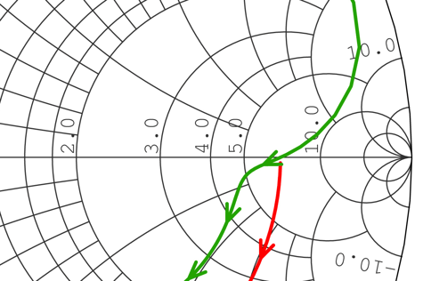
Smith Charts, shown in figure 1 below, plot antenna impedance against operating frequencies. They are a useful visual tool for solving impedance mismatches.
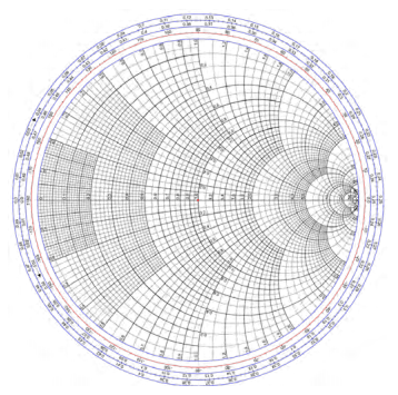
Figure 1: Smith Charts used to solve impedance mismatches.
Fortunately, product designers no longer have to rely on Smith Charts or complete the complex calculations required to complete impedance matching manually. There is a free calculator for GCPW transmission lines that completes the calculations at a mouse click.
Using Pi networks for impedance matching
Designers have additional options for impedance matching using established RF circuit designs. The basic impedance-matching circuit is called an L-network and there are four variations. The most common impedance matching challenge met by an L-network is matching antenna impedance to the receiver input, or the transmitter output.
However, this configuration does not work with wideband applications. An alternative configuration is the π-network. These are called π-networks because they are essentially two L networks that together look like the Greek letter pi. The objective of the π-network is still to match the impedance of a load to a source. But with the additional components, a π-network is flexible enough to work with almost all applications.
.jpg?width=636&name=impedance-transformations-l-network-matching-topologies%20(1).jpg)
Figure 2: Impedance transformations for L-network matching topologies
Conclusion
Impedance matching is a vital element of designing the circuits for any product that incorporates an embedded antenna. The theory behind impedance matching and how to calculate the correct component specifications is complex. However, designers have a range of standard tools, including both calculators and standard circuits, they can use to optimise the performance of the embedded antennas in the devices they design.
For more complex devices with multiple embedded antennas, Antenova offers a circuit design and consultancy solution. By designing your PCB with optimal impedance matching across all the components, your device will operate at maximum power and effectiveness. Contact us to find out how you can optimise the performance of your RF and wireless product design.