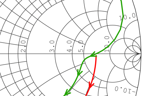
If PCB board design itself is highly complex, impedance matching is a dark art. With all the time and expertise that go into finalising a design; ensuring antenna impedance is correctly matched to source impedance can be daunting, especially when faced with complicated equations and a Smith chart – pictured below.

The traditional Smith Chart method requires a comprehensive understanding of the principles of RF, and involves a variety of steps. When designing very small devices, that require feed lines to navigate tight spaces and multiple components; the Smith chart method can prove challenging.
A Smith chart performs a necessary step in calculating the matching component values of your device. Calculating the impedance of an antenna, while vital to the effective operation of a wireless device, needn’t be so challenging. Impedance continuity allows an antenna to radiate at the intended frequency with minimal deviation, vastly increasing a devices performance capabilities.
An unmatched antenna will suffer a significantly reduced range and may render the device unable to operate effectively. This can cause issues such as reduced battery performance, poorer load speeds, or lack of signal.
If your device is defective due to an antenna impedance miscalculation, the manufacturing process can be greatly delayed; leading to unanticipated costs, lengthy redesigns and even entire product recalls.
Impedance matching the easy way
For effective impedance matching, it is necessary to alter your transmission line dimensions. Beneficial, is to utilise grounded coplanar waveguide transmission lines. This is because their dimensions - including the width and the gaps between the feed lines conductors, as well as their height - can be altered to ensure impedance continuity between the antenna and its source.
Additional benefits to using GCPW feed lines include:
- Additional RF grounds keep the feed best isolated from any interference
- Low inductance for shunt elements
- Lower loss performance at higher frequencies (required for 5G)
- Can narrow arbitrarily to navigate tight spaces
- Match component width with PCB trace width to save real estate
- Achieve low impedances
Antenova's Transmission Line Calculator
Due to the additional feed track dimensions, matching impedances via GPCW feed lines is a complex process. At Antenova, we recommend using our new free impedance matching calculator as it enables designers to quickly calculate the optimum dimensions of their transmission line to ensure efficient performance.
Antenova’s new tool is designed to be easy-to-use, and calculate dimensions quickly and accurately. With greater speed and accuracy, designers are able to tune the dimensional characteristics of any feed line without having to compromise on the PCBs design.
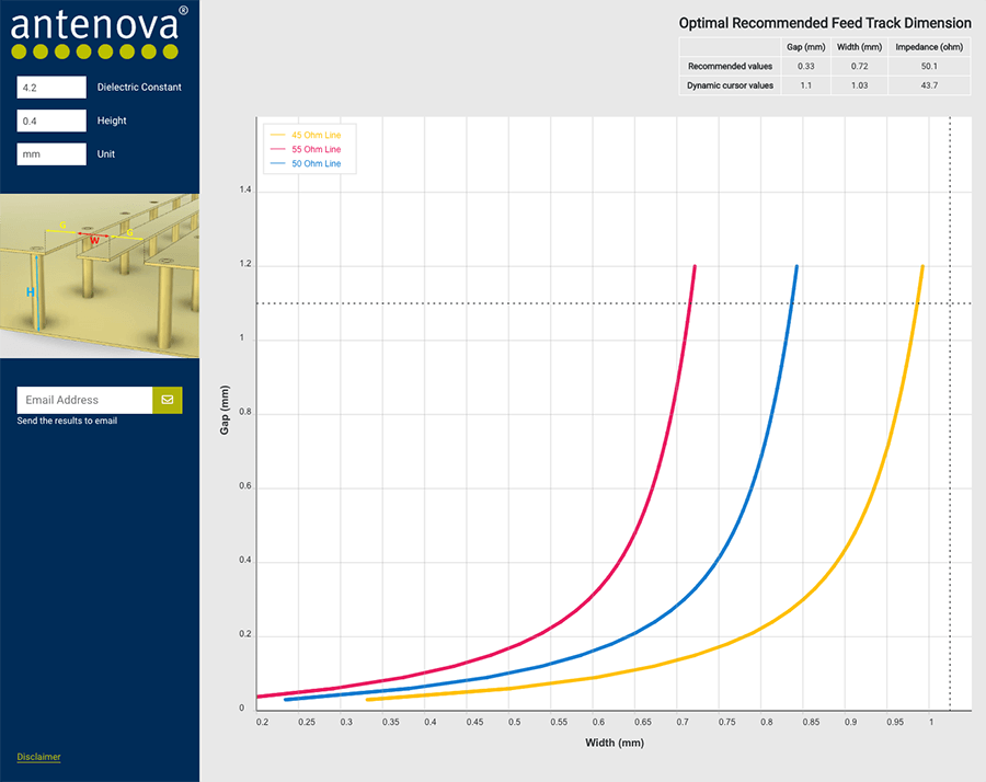
To use our transmission lines calculator effectively, follow the instructions below:
- Set dielectric constant to the FR4 specification (a typical value is 4.2 for FR4 which is the default value).
- Select your units of measure either mil or mm (mm is the default setting)
- Select the Height between the top layer and the desired internal GND layer of your PCB. This is dependent on your PCB stack up. The default value is 0.4mm but you should set the actual value of your PCB as this is a large determining for the feed dimensions.
- The result is live once you change the input values of Height and the Dielectric constant. A table is shown which gives dimensions for the feed Gap and Width based on 50ohm using nominal ranges for the size of the trace width and gap. However, if you require to use smaller or larger traces than given you can simply move the cursor over the generated graph to select the values best suited to your design.
- The graph has three lines where blue is the 50ohm line. A tolerance of + and – 5 ohms lines are shown as they are the acceptable limits for a feed construction. Ideally you need to stay with values given within these lines to ensure a good low loss feed.
With all the possible options mapped out, the designer has the flexibility they require to ensure feed line dimensions match the source and load impedances, while being best-suited to their PCB board design.
For designers, working to get very complex PCB boards ready for that all important testing stage, this free and easy-to-use tool is hugely liberating. It takes the stress and risk out of a process that can otherwise be time-consuming and complicated. That means one less thing to worry about, and peace of mind when it comes to calculating antenna impedance. In doing this, the calculator helps ensure that your device performs as it should, and receives the full benefit of any chosen antenna.