Today's Internet of Things (IoT) devices may be small, but they pack a strong wireless punch. Within a tiny form factor, they contain vast amounts of technology and impressive features. It's enough to make the technology of even a few years back look antiquated by comparison.
Semiconductors and integrated circuits (ICs) are smaller and more compact than ever before. Owing to these advances in technology, tiny wireless devices have exploded onto the market. Yet wireless components and RF circuitry can only shrink so much, as they are bound by the laws of physics. Undeterred, many designs still seek to push the envelope of possibility. Many of these efforts succeed, like the slim smartwatches and tiny trackers in use today, a lot though, do not. There are countless examples of products that failed network certification and perform poorly, and all at great expense.
There are very few reasons why a wireless product cannot be both small and powerful, as long as the laws of electromagnetics and physics are observed carefully. This makes selecting the right components and carefully reviewing their integration is critical. Thoroughly reviewing Gerber files can help identify and troubleshoot issues before they manifest in prototypes, or, heaven forbid, a mass manufactured product.
What value does a Gerber review bring to a wireless project?
Gerber files are rendered footprints of a PCB stackup. Considering the costs involved in rectifying an issue with already printed circuit boards, it is an easy process to introduce before any files are sent for manufacture, so it is a great way to insure against errors.
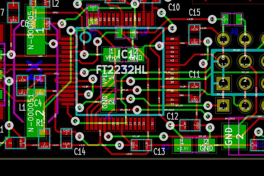
One of the most important, yet understated, aspects of a wireless stackup are the RF transmission lines. These are the traces that carry RF energy from an antenna through to wireless modules and the like. The reason why these are so important to optimise, is that signals could be emanating from kilometres away, yet a sub-optimum transmission line design could be reflecting these signals back into the antenna – after they are received. This creates unwanted noise and potentially detuning. Blockages can be measured during antenna tests for VSWR (voltage standing wave ratio), a measure of reflection coefficient. Many issues relating to VSWR can be traced back to the initial design confirmed during the PCB layout.
Software packages for Gerber reviews
Gerber files provide the perfect format to visually inspect and review important elements of an RF stackup, including transmission lines.
There is no shortage of programs that allow you to view these files. There are free versions, like ViewMate, which mimic the CAD manufacturing software used by printed circuit board producers. Most software packages allow you to measure and review distances between your transmission line and other components, as well as the dimensions of the transmission line itself. Popular paid CAD designers like Altium Designer are also fully capable of allowing Gerber file-like reviews. Essentially, any software package that allows you to visualise your PCB layout will allow you to check for RF design issues. It is important to note though, some software packages do not support the use of grounded coplanar waveguides.
Once you’ve selected your preferential software, there are some essential things that you will want to check for in regards to RF.
The Gerber file review checklist
There are a range of factors to consider when reviewing your PCB layout for wireless performance. The following list is a brief overview of the themes and major factors to check throughout and after design. Remember, RF, wireless certification and wireless product design experts may identify particular features of your design not covered in this list.
For a more rigorous review, check with your antenna manufacturer, as many provide free Gerber file reviews for customers. If you have designed in an embedded Antenova antenna, get in touch with your local representative to get your files reviewed. When submitting your file, include a written document that details information about the PCB stackup, materials and layer thicknesses of your PCB, as these all play a role in determining performance.
Is the choice of transmission line suitable for the device?
Both microstrip and grounded coplanar waveguides (GCPW) are popular choices of transmission line for high frequency radio communications. In a compact or miniaturised design, a GCPW transmission line will likely deliver better performance for two main reasons.
Firstly, they provide an unbroken ground plane, required for effective performance for ground-plane dependant embedded antennas. The ground plane should be positioned on the opposite side of the dielectric material of the PCB.
Secondly, the grounded layer provides greater isolation for the transmission lines and thus RF energy, which in turn reduces losses and reflections.
However, many CAD programs fail to properly support them. Combined with a lack of knowledge and awareness of their benefits, this often means microstrips are used where a GCPW would provide superior RF performance. At the early stages of a design, the benefits of both of the two recommended transmission line types should be considered.
Are the dimensions of the transmission line optimised?
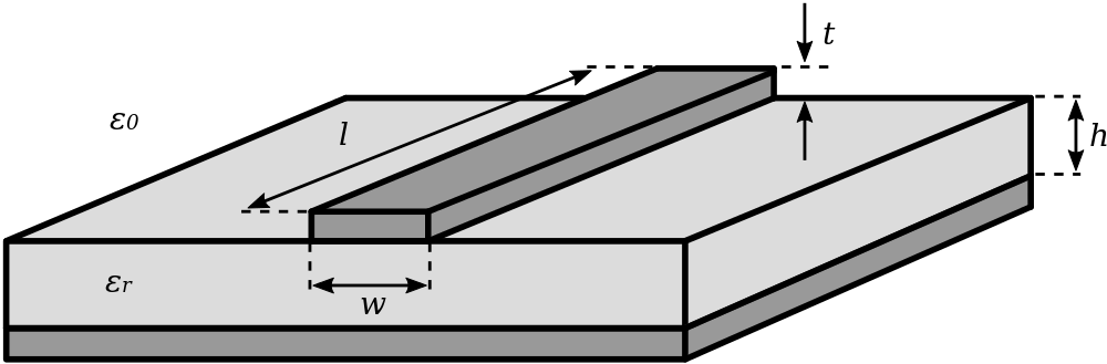
One of the features of a transmission line is that their dimensions can impact performance. Like all RF circuitry, components and transmission lines should be tuned to operate at a characteristic impedance of as close to 50Ω as possible.
There are many online calculators available that allow designers to plug in dimensions (H, T, A and B, as well as the relative dielectric constant) into the tool and the tool will provide an estimated characteristic impedance. Note that these tools are based on rudimentary calculations and the results can vary based on the way the tool is coded. Where possible, use the manufacturers calculators or contact the antenna vendor to be sure.
Also, consider that thinner RF transmission lines generally contribute to lossier performance; closing off yet another miniaturisation avenue.
Other factors to review
Other common issues include:
- Transmission line corners and bends. If it’s necessary to corner a transmission line, the line should be cornered through a rounded edge or a chamfered corner – avoid right angles where possible, as these increase losses.
- Vias: spacing and placement. Near RF circuitry, vias contribute to RF performance, as they help reduce ground inductance and can mitigate against unwanted coupling.
- PCB materials. Low quality FR4 circuit boards can cause mismatches and other RF issues which may only become apparent after production. Ask to inspect samples from your PCB manufacturer if you are at all worried.
An opportunity not to be missed
From spurious emissions and higher VSWRs, all the way to network certification rejection, the cost of a poorly optimised RF stackup can be devastating. This makes the argument for integrating a gerber file review process within your design cycle even stronger.
Antenova recognises this. Customers are offered complimentary gerber file reviews, so there’s no reason not to take them up on this offer. Other antenna manufacturers offer this service too, although many charge a fee. Doing this may save you a heap of money and time later down the line.
Of course, there’s always your peers which you can ask, too. If you have any questions or suggestions about the recommendations made in this article, feel free to comment or pose your own answers to questions through our forum.